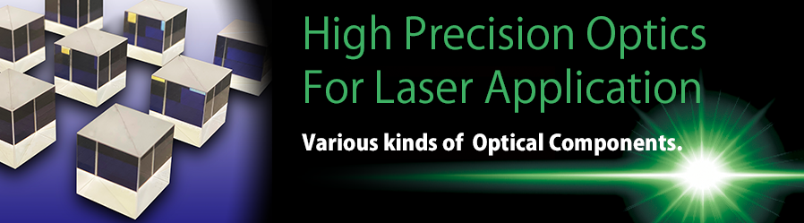
We provide high-precision optics for required in the laser field, such as High Reflectance Mirrors, Optical Filters, Optical Prisms and various kinds of Optical Components.
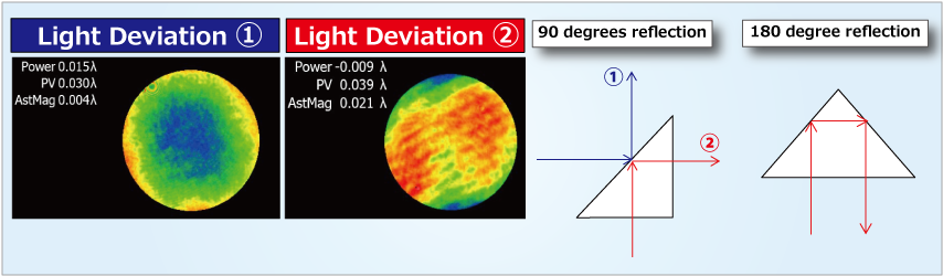
Right Angle Prism

Using for reflecting the Incident Light to be altered 90 or 180 degrees. All Light reflects on the reflective surface because the total reflection happens.
AR coating is applied to the incident and exit surface depending on the application.
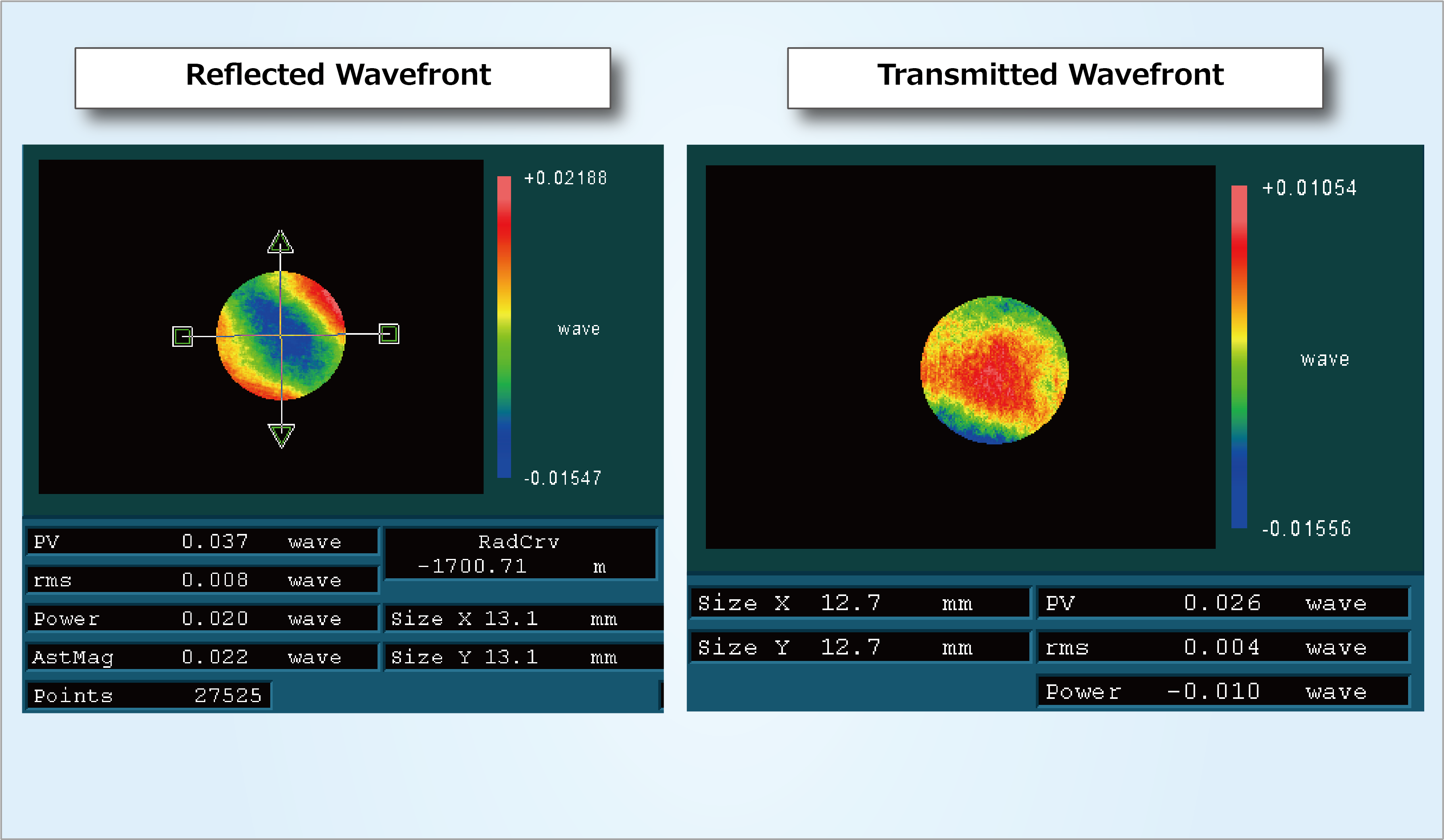
We can supply high precision transmitted wavefront by precisely controlling polishing and thin film coating.
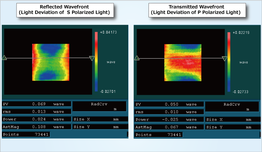
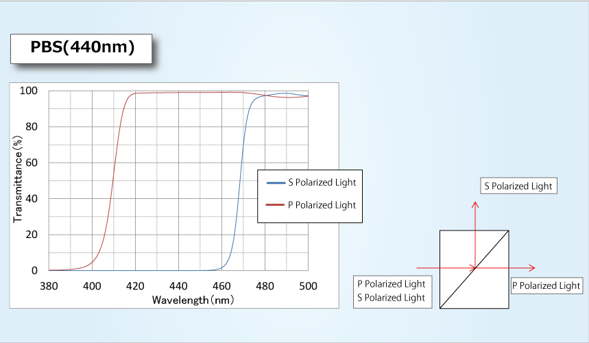
Polarizing Beam Splitter

Using for separating the polarization of incident light. P polarized light transmits and S polarized light reflects in the 90 degree direction.
AR coating is applied on the exit surface and polarized light is applied on the slope.
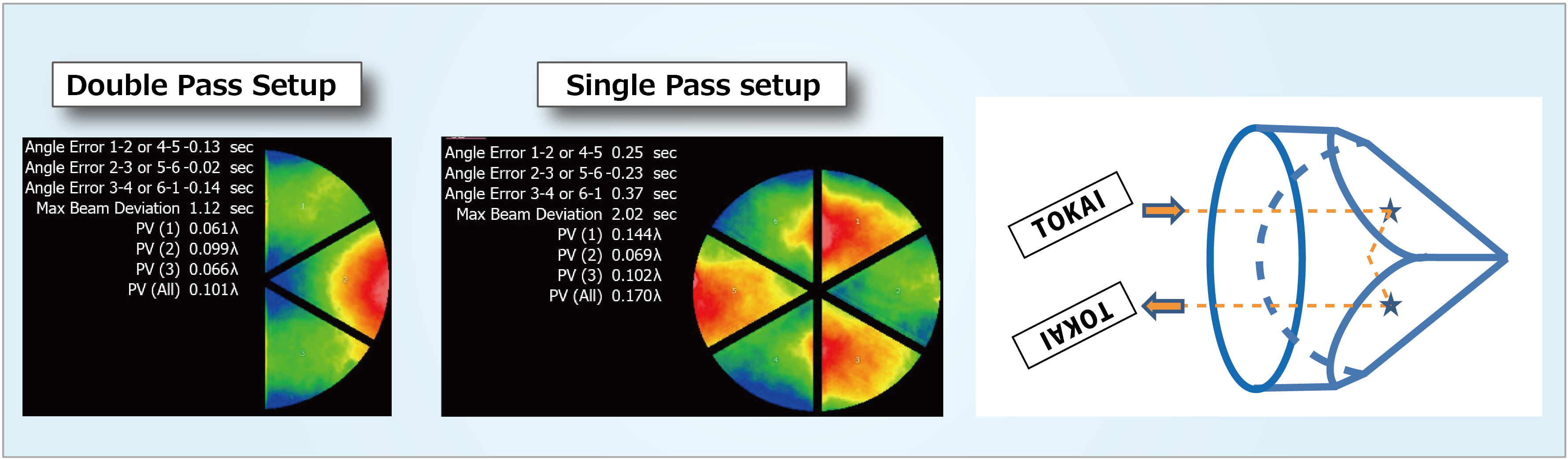
Corner Cube Prism (Retroreflector)
Using for returning all incident light to the incident direction. Light Angle Deviation: 3″ Max. High reflectance silver deposition and black protective paint are applied to protect the reflective surface from dirt. AR coating on the incident surface can be customized from the visible to the near infrared to match the light source used by customer.
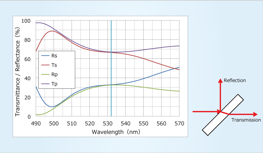
Beam Splitter
The purpose of beam splitter is used to separate the incident light. We apply to be coting according to applications such as polarization separation, and light intensity separation.
In addition, we supply high precision wavefront distortion both transmitted and reflected light.
_english.jpg)
_english.jpg)
_english.jpg)